PDP-11 Line Time Clock Repair

The KW11-L is an option card for the pdp-11/40 that adds a 50/60 Hz clock. It can be configured in a polling mode or interrupt mode.
Symptoms
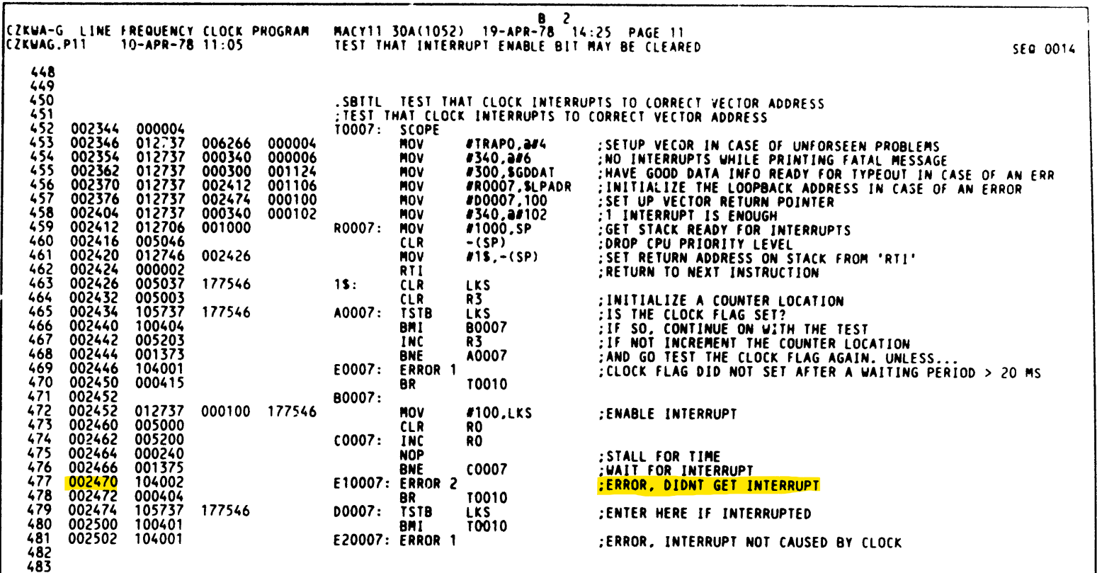
When running the KW11-L diagnostic software (ZKWAG0), one of my two KW11-L cards would fail very early on in the tests. Specifically, the test would stop at address 002470, in the listing that is "ERROR, DIDN'T GET INTERRUPT", clearly, something was fundamentally wrong.
Initial Theory
Clearly, whatever is wrong is fundamentally important to the basic operation of the KW11-L. The two most obvious areas of possible failure are the bus interface or the circuitry responsible for triggering the interrupt. My other card confirms that the processor is at least partially functioning and is unlikely to be a fault.
Personally, I'm more inclined to point my finger at the bus interface as it's significantly more complicated than the logic to trigger interrupts.
A Note on Unibus Faults
The logic that implements the Unibus interactions can be thought of as a state machine. When it is operating correctly, the Unibus logic will set and clear several internal and external flip-flops (they hold various bits of state), ultimately returning to the same state as they started.
However, when the bus logic is malfunctioning, various state flip-flops will often not get set or will not get cleared. By examining the state of the various unibus flip-flops, we can gain an understanding of where the unibus transaction got stuck!
Investigation
Line Clock Signal
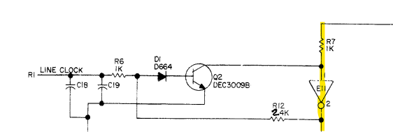
It's best to start with the simplest things first; for that reason, I started my investigation by verifying that the 50Hz line clock signal was making its way into the card. It only took a couple of minutes of Investigation to verify that the LINE CLOCK was making its way to the board without any issues.
Unibus Interface
As I explained previously, it's always worth looking at any flip-flops that are involved with Unibus transactions. In the case of the KW11-L it has 5 such flip-flops.
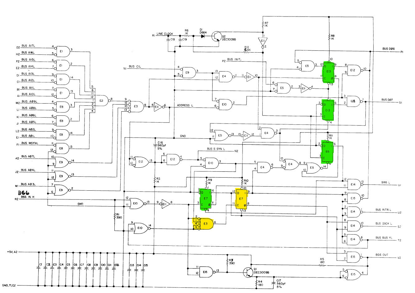
I spent about 15 minutes looking at all 5, some would set and clear, while a couple would set and not clear. Notably, E7 was not being reset at the end of the Unibus transaction. Working backwards down the clear line found E3. Checking the inputs and outputs of E3 was it was apparent that E3 wasn't working!
The Fix
While reviewing the schematics, I noticed that E3 is labelled as a "DEC 8815." You might be asking, "What’s a 8815?"—I was wondering the same thing. Googling turned up nothing so I had to try and work it out from the schematics.
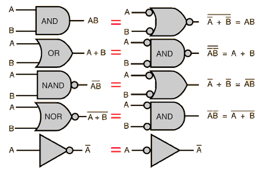
Scanning over the schematics, I only found two gates belonging to E3, two 4-input-and gates with inverted inputs. Doing a little bit of research for other 4-input logic gates, I quickly realised that the pinout of the 8815 matches that of the 7421 Dual 4-Input AND gate. But that is an AND gate, it's missing the inversion on the inputs. Fortunately, a NOR gate is logically equivalent.
Refining my search for a replacement, I found the 7425 Dual 4-input NOR Gate. It's almost a perfect replacement, except the 7425 has an additional signal, "strobe" (active high output enable). Luckily for us, the signal is active high, so we can simply leave those two inputs floating and the chip will function as we need it to.
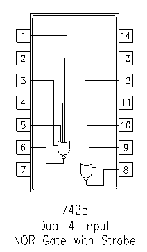
Note that the 7425 may not be a perfect replacement for the 8815. Without the data sheet for the 8815 we can't be sure. Also, make sure that pins 3 and 11 aren't connected to something if you need to replace an 8815 yourself.