PDP-8/e RX8E Repair

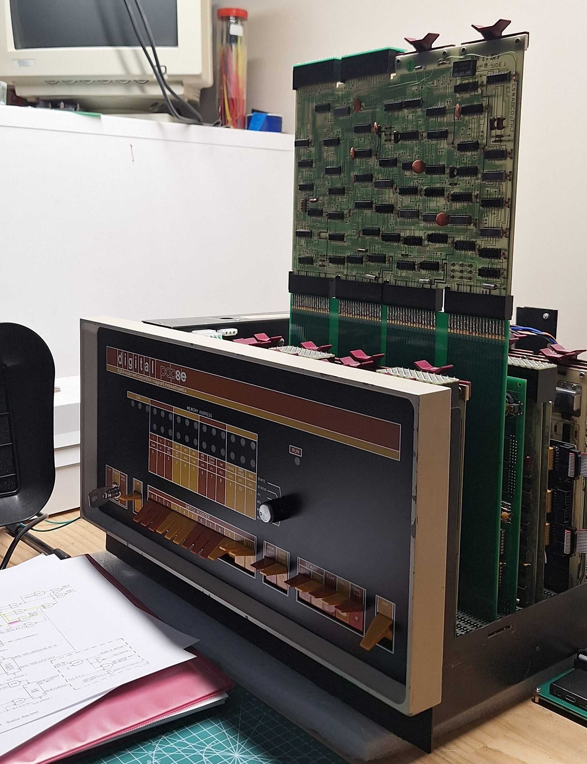
I have on the workbench three RX8E PDP-8 RK05 controllers. The goal is to get all three sets 100% working. After doing some initial testing and swapping of boards, I have come to the disappointing conclusion that no combination of boards is fully functional.
Repair Strategy
Having three sets of boards is a massive advantage; the RX8E is rather complex, having its logic poorly distributed over three cards.
Firstly, I am going to identify the combination of cards that results in the longest test run time. Then I am going to test each board type from each set. I will then fix the board that fails the test the fastest.
Board: M7106, Set 1 - 1s - 2026/09/10
STATUS REGISTER ERROR
PC:0243 GD:2200 ST:2202
This board failed its test in under 1s. We can see from the PC that it only got 43 instructions into the diagnostic before it failed.
Expected value: 2200
Received value: 2202
The error shows that bit 10 was 1 when it should have been 0; the other bits are correct. Looking at a block diagram, we can see where bit 10 is coming from.
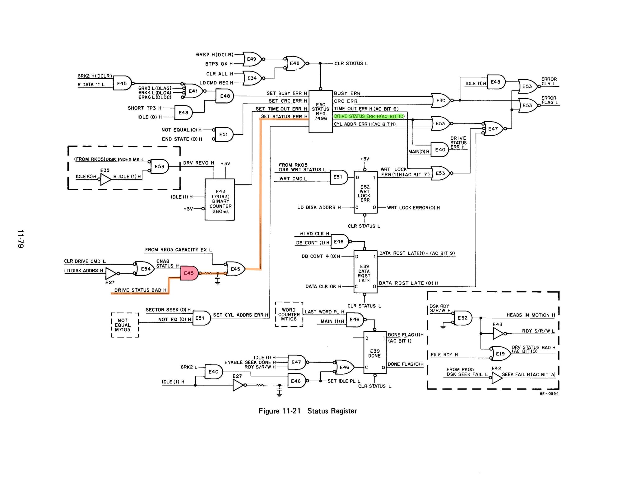
Looking at the circuit with the oscilloscope, I found that E45 was bad and was putting out 2v constantly. Replacing the 7408 fixed the issue, and the card works as well as the other two.
Board: M7104, Set 1 - 3s - 2026/09/20
This board made it to test 3 before a fault was found and ran for 3s.
COMMAND REGISTER ERROR
PC:0264 GD:0000 CM:0407

Expected value: 0000
Received value: 0407
Test 3 reads the command register and checks that it's 0. The register is expected to be initialised to zero when the computer boots and when the CLEAR key is pressed. In this case, and every time I run the test, it returns 0407 when trying to read the command register.
The command register is not a general-purpose read/write register; reading it is rather involved and is done via the maintenance interface. It took me quite a bit of time to understand the method. Here is a listing for a program to do it:
    /READ COMMAND REGISTER                                              Page 1
    1              /READ COMMAND REGISTER
    2        0020  *0020
    3 00020  0206  XRDCM, RDCM
    4 00021  0224  XMAIN2, MAIN2
    5 00022  0233  XLDMN, LDMN
    6 00023  7764  M12, -14
    7 00024  0020  K0020, 0020
    8 00025  0400  K0400, 0400
    9 00026  0000  SBCNT1, 0
   10 00027  0000  CMREG, 0
   11
   12        0200  *0200
   13              /
   14              / MAIN
   15              /
   16 00200  7200          CLA                 /CLEAR AC
   17 00201  7001          IAC                 /AC=0001 (SIMULATE A POWER CLEAR)
   18 00202  6742          DCLR                /CLEAR ALL (DCLC)
   19 00203  4420  TST3,   RDCMD               /READ COMMAND REGISTER (CM in CMREG & AC)
   20 00204  7402          HLT                 /HLT
   21 00205  5204          JMP .-1
   22              /
   23              /SUBROUTINE TO SHIFT COMMAND REGISTER TO
   24              /DATA BUFFER THEN READ DATA BUFFER
   25              /
   26 00206  0000  RDCM,   0
   27 00207  4421          ENMAN2              /ENTER MAINTENANCE MODE+DB41
   28 00210  1023          TAD     M12         /LOAD MINUS 12 (7764)
   29 00211  3026          DCA     SBCNT1      /12 BIT SHIFT (SAVE COUNTER)
   30 00212  1025          TAD     K0400       /ENABLE BIT FOR SHIFT COMMAND (MR=6000+0400) (CHECK COMMAND REGISTER)
   31 00213  4422          LDMAN               /LOAD AND GO (SHIFT  COMMAND REGISTER TO DATA BUFFER4)
   32 00214  2026          ISZ     SBCNT1      /INCREMENT AND SKIP IF ZERO
   33 00215  5213          JMP     .-2         /SHIFT 12
   34 00216  7300          CLA CLL             /AC=0, L=0
   35 00217  1024          TAD     K0020       /ENABLE TRANSFER CONTENTS OF DATA BUFFER 4 TO THE AC (MR=6400+0020)
   36 00220  4422          LDMAN               /LOAD AND GO
   37 00221  3027          DCA     CMREG       /SAVE AC (COMMAND REGISTER)
   38 00222  1027          TAD     CMREG       /RESTORE IT
   39 00223  5606          JMP I   RDCM        /RETURN FROM SUBROUTINE
   40              /
   41              /SUBROUTINE TO ENABLE MAINTENANCE MODE
   42              /SET DB4=1 TO ENABLE SHIFT TO LOWER SILO
   43              /
   44 00224  0000  MAIN2,  0
   45 00225  7330          CLA CLL CML RAR     /ENABLE SET MAINTENANCE MODE (AC=4000, L=0)
   46 00226  4422          LDMAN               /LOAD MAINTENANCE, SET ENABLE (MR=4000)
   47 00227  7010          RAR                 /ENABLE SET DB4=1 (AC=2000)
   48 00230  4422          LDMAN               /LOAD MAINTENANCE, SET DB4=1 (MR=6000)
   49 00231  7300          CLA CLL             /AC=0, L=0
   50 00232  5624          JMP I MAIN2         /RETURN FROM SUBROUTINE
   51              /
   52              /SUBROUTINE TO ISSUE "DMAN" MAINTENANCE IOT
   53              /
   54 00233  0000  LDMN,   0
   55 00234  6747  IOT7,   DMAN
   56 00235  5633          JMP I LDMN
   57
   58        6747  DMAN=6747
   59        6742  DCLR=6742
   60        4420  RDCMD=JMS I XRDCM
   61        4421  ENMAN2=JMS I XMAIN2
   62        4422  LDMAN=JMS I XLDMN
   63                      $
Essentially, one of the maintenance functions allows the command register to be shifted into Data Buffer 4, one bit at a time. Once the data is fully shifted, the user can then read Data Buffer 4 into the AC.
Actually, quite a large portion of the hardware is required to be functioning correctly to run this simple test: instruction decoding, maintenance functions, maintenance register, bus interface, shifting logic and power-on reset logic. Surprisingly, this is the second test; I would have had other tests before this one.
Initially, it took me quite a long time to figure out how reading from the Command Register works, but it's actually quite simple. It's just that the explanation in the documentation isn't so good.
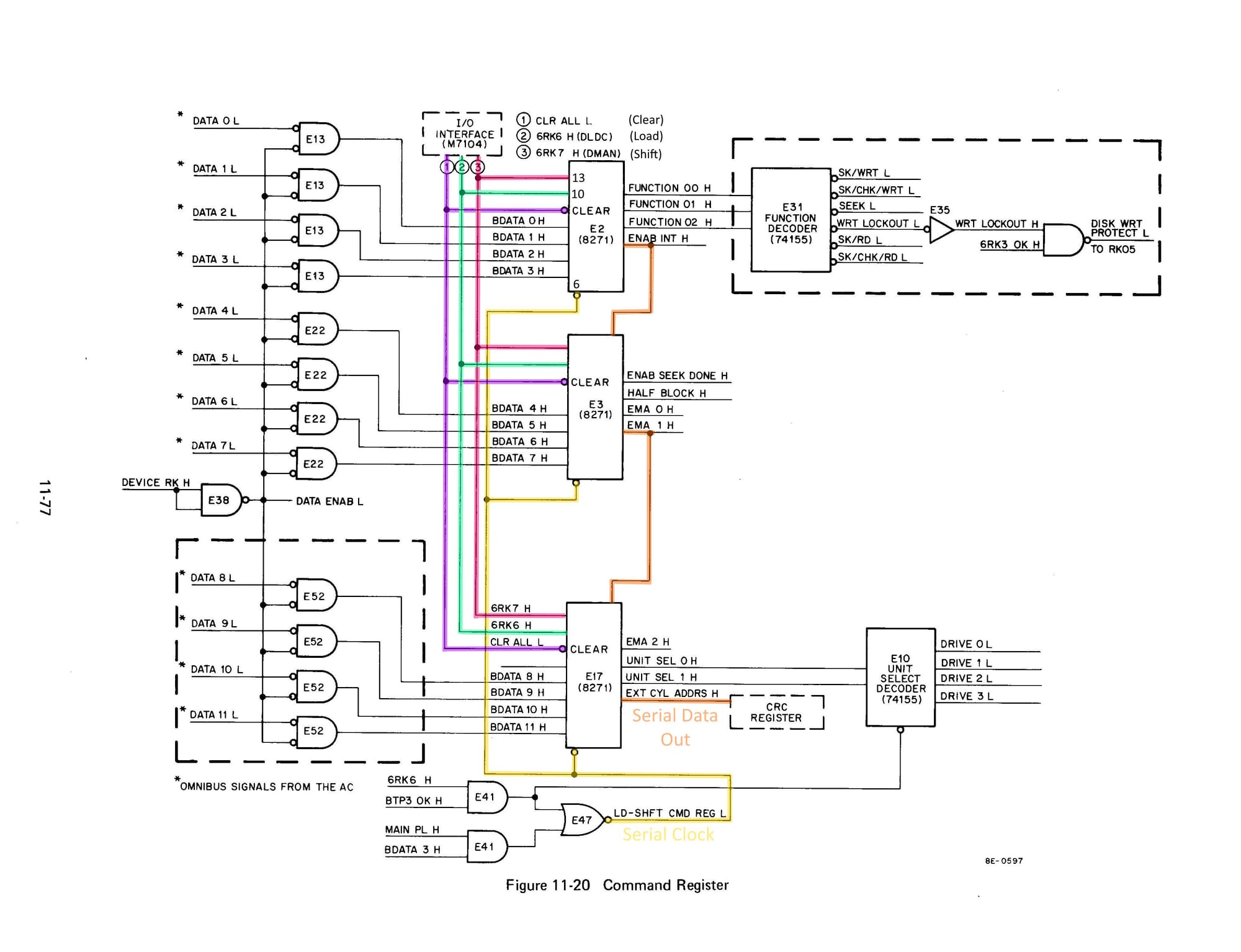
First, the Command Register is constructed from shift registers. This lets it function as both a register and a shifter. When we want to read the Command Register, we shift its content out via "EXT CYL ADDRESS".
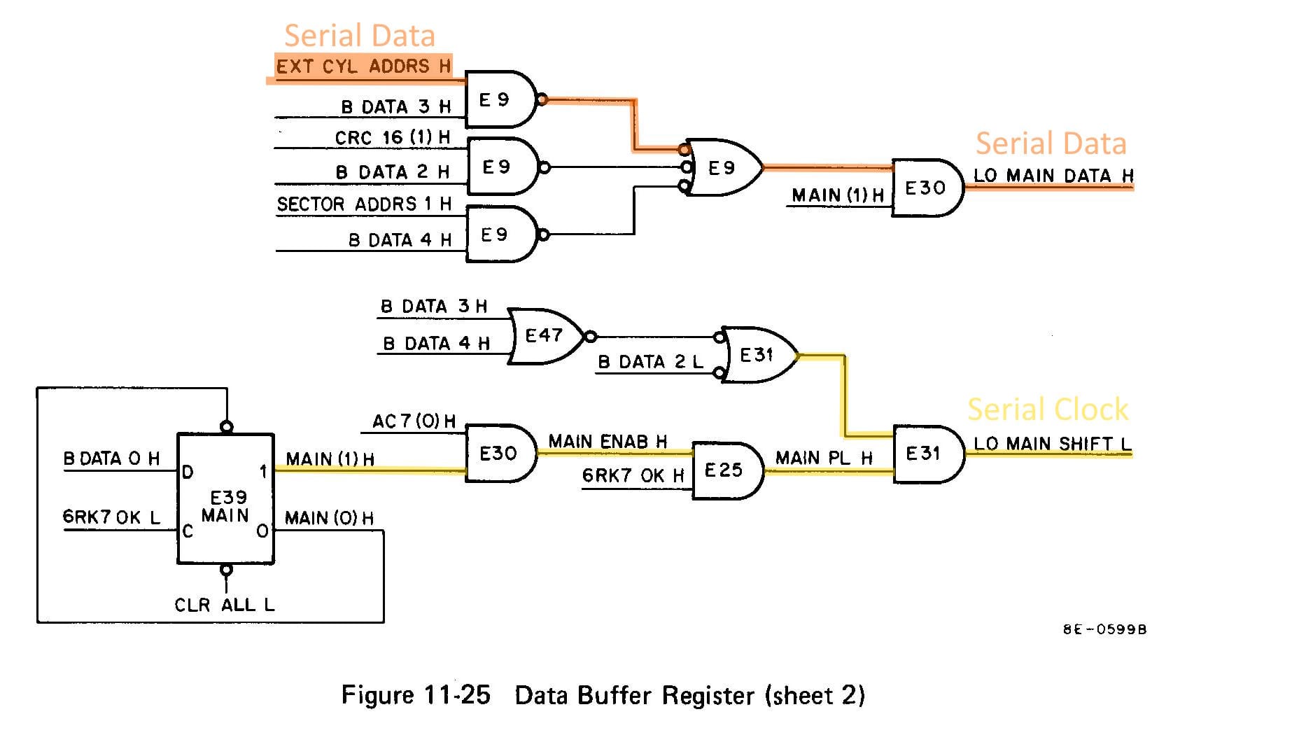
The data makes its way out, goes through some controlled gates and gets a new name: "LO MAIN DATA H". At the same time, we also construct the serial clock "LO MAIN SHIFT", which is used to shift the serial data into Data Buffer 4.
Finally, the data makes its way into the Data Buffer Registers. It's clocked in and shifted through the Data Buffer 4 register. The 7495 shift register can be parallel or serial loaded; decided by the Mode Switch input. The output from Data Buffer 4 eventually makes its way back to the AC through the various muxes and gating logic.
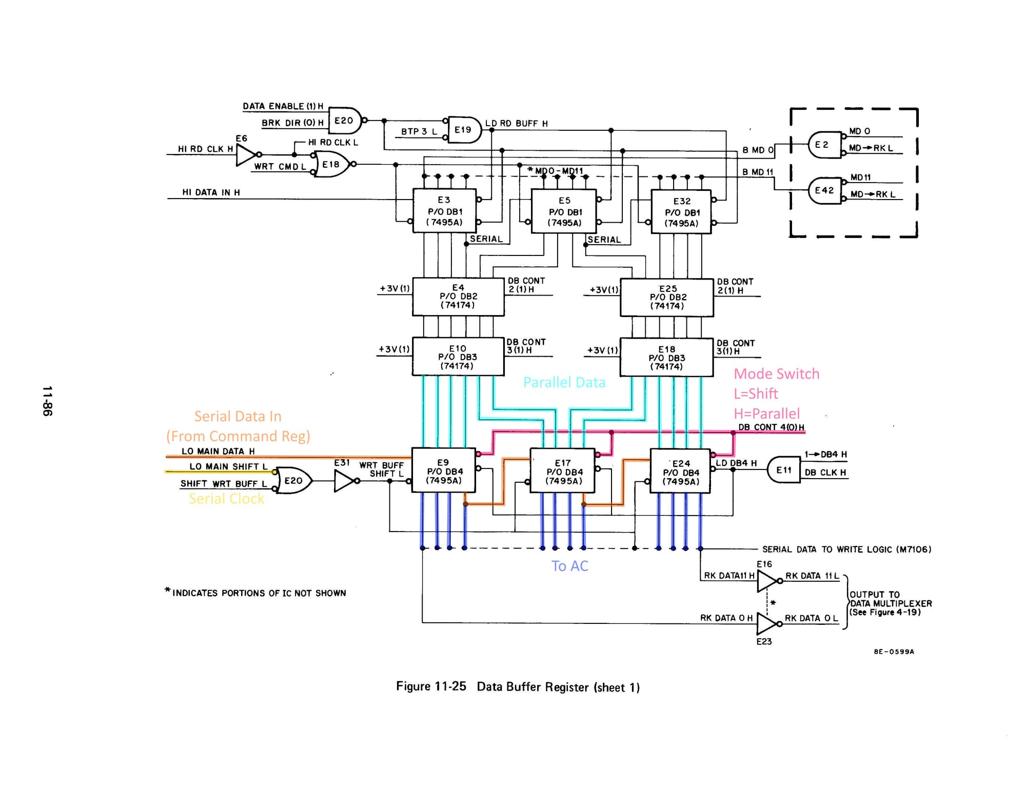
Having spent a day and a half figuring all of this out, it was time to track the error down. Starting with the, I ensured that the serial clock was present and that data was being shifted out. In this case, the Command Register was empty, so it was just a stream of zeros.
Moving on to Data Buffer 4, I started with the serial clock and serial data; both were present. Next, I checked the Mode Switch, and this is where I found the issues. "DB CONT 4(0) H" was at 2V; following it back, I found a JK flip-flop. All outputs for the flip-flop were at 2v; very clearly, it was broken. Replacing the flip-flop fixed the problem.
In summary, a bad input to the Data Buffer 4 was causing it to load data from the parallel input rather than its serial input, producing totally wrong results.
Board: M7106, Set 2 - 3s - 2026/09/25
This board failed at test 15, a test of the sector register. In hindsight, the failure was fairly obvious.
DISK ADDRESS REGISTER ERROR
PC:0515 GD:0000 DA:7740

Expected value: 0000 (000000000000)
Received value: 7740 (111111100000)
The Surface/Sector register is 5 bits wide and implemented with a 7496 5-bit shift register. Just like the Command Register, it's possible to shift the data out using maintenance mode into Data Buffer 4. This is exactly what test 15 does.
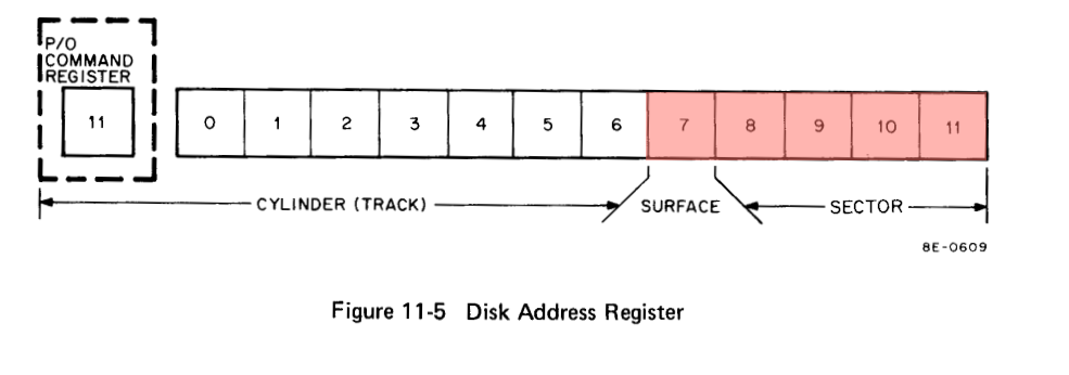
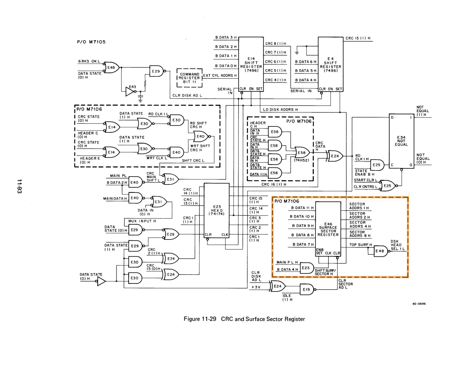
Surface/Sector uses a lot of the same logic as the Command Register, so from previous experience we have a reasonably good idea of how it's meant to be shifted into Data Buffer 4.
The first step is to verify that the correct data is being loaded into the Surface/Sector register. After writing a test program, it was simple to confirm that the register was being loaded correctly.
Next was to check if the data was being clocked out of the register. Looking at the scope, it was clear that the data was being shifted out, but something did not look right. Doing side-by-side comparisons with another board, the issues became immediately apparent. In the case the serial input pin had failed, this caused 1's to get clocked into the register rather than zeros.
If I had been more careful looking at the logs, it may have given me a hint that this was happening. From the test, we can see the data we received was 111111100000. You may notice that the first five bits are zero, as they should be, while the others are 1, whereas they should have been 0. Replacing the 7496 fixed the issues, and the test passes.
Connector Block - 2026/09/26
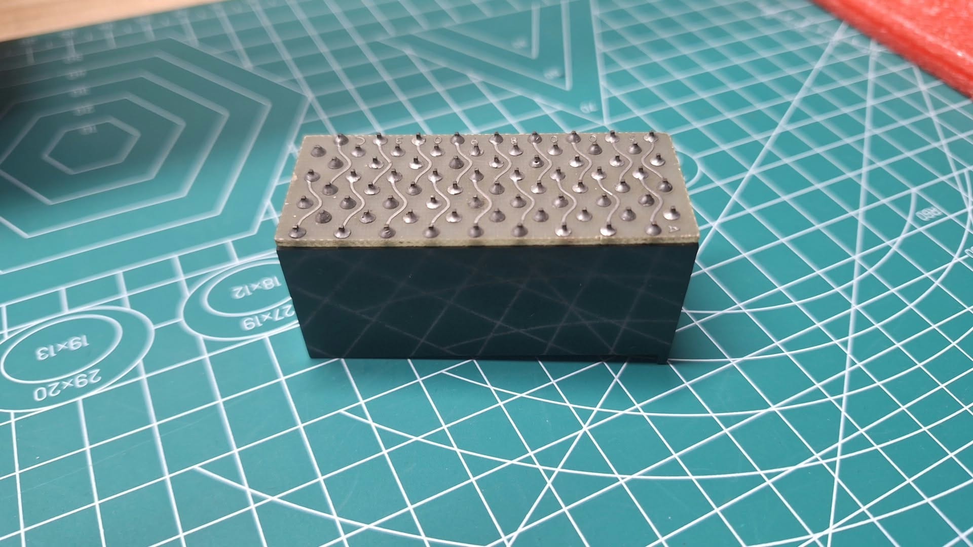
When searching for the next card to fix, I found that all the cards were stopping on the same error. That indicated there was a common fault, possibly the CPU or possibly something mechanical. So I started with the simplest thing first and switched to another set of connectors, and found that one of them did not work.
Up until this point, I have been careful to use the same blocks in the same order; evidently, this was wise. Had I been a little bit more unfortunate, this may have been an extremely difficult problem to track.
Examining the connector block, it looks as if the solder hasn't flowed to the reverse side of the PCB. Approximately 5-6 of the pins are not connected properly at all. Presumably, the original users of the controller had a lot of difficulty.
Board: M7106, Set 2 - 43s - 2026/09/26
Test27 - Verify That Write Lock Inhibits Load Address. - This was a nice and simple fix.
The RX8E allows the write protect to be enabled on the RK05 Drive; once this is done, it blocks all changes to the Address Register. In this case, the test result indicated that this wasn't working properly.
DISK ADDRESS REGISTER ERROR
PC:1055 GD:0000 DA:7776

Expected value: 0000
Received value: 7776
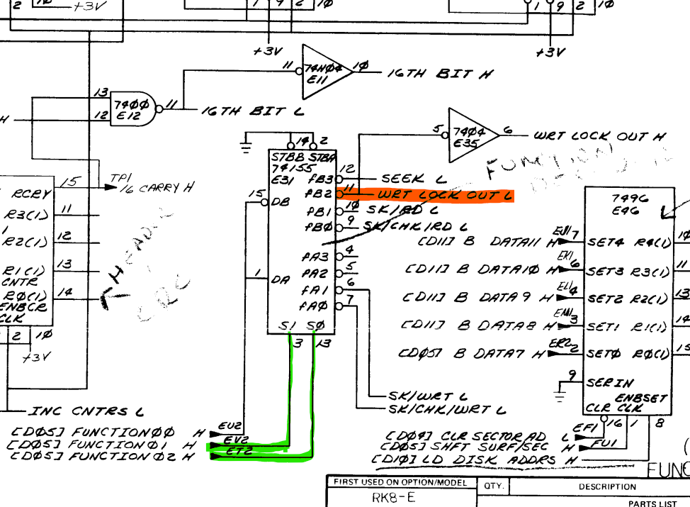

The circuitry for this function is very simple. Write Lock Out is developed from the Commander register via a 74155 mux. Write Lock Out then goes on to gate the LD DISK ADDRESS signal. In this case, the mux chip had failed and Write Lock Out was never generated. Replacing the 74155 with a 74LS155 fixed the issues. I will order some 74155 chips.
Board: M7106, Set 2 - 1:20s - 2026/09/27
This fault was difficult to track down but easy to understand. Test 36 uses the maintenance function to shift AC10 into the CRC Register, then reads it back.
CRC REGISTER ERROR
PC:1341 GD:000000 CR:177777

Expected value: 000000
Received value: 177777
After doing some testing, I observed that 16bits of data did look to be shifted in and out. However, the reason the test was failing was that 1s were being loaded into the CRC Register even though 0 was requested.
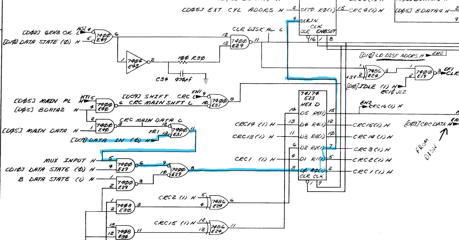
Working back from the input to the shift register, we see that MAIN DATA (maintenance data, AC10) is gated by several control signals. In this case, the signal of note is "DATA IN (0) H".
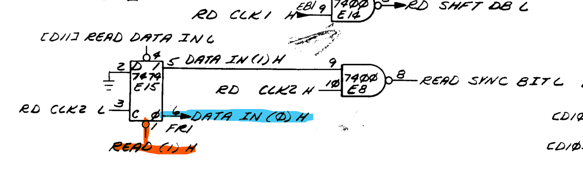
"DATA IN (0) H" comes from a flip-flop, the output of which was ok but wrong for the needed operations. Looking at the inputs, I notice that pin 1 was at 2v, it definitely shouldn't be.
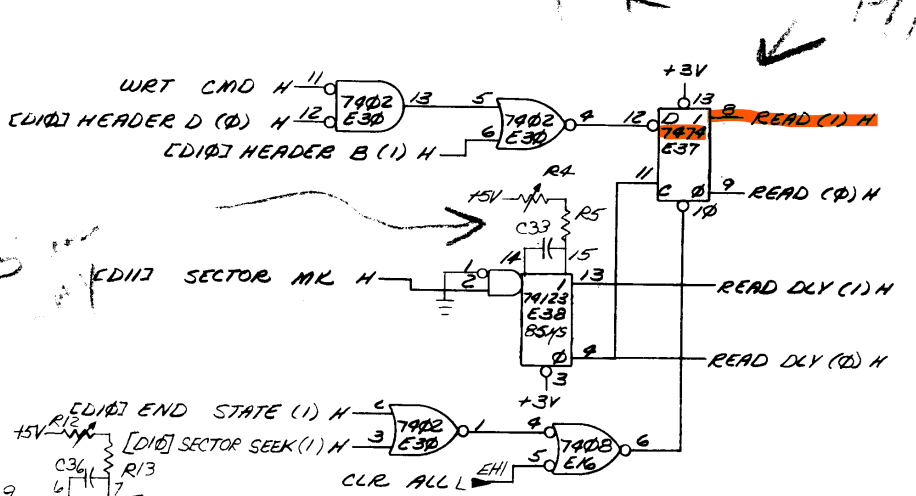
Moving back once more takes us to another flip-flop. It was defective and the source of the 2v input to the Data flip-flop. Replacing the flip-flop fixed the issue.
Board: M7104, Set 3 - 1:20s - 2026/10/2
DATA REGISTER ERROR
PC:1543 GD:7777 DB:0000

Expected value: 7777
Received value: 0000
This test works by serially loading DB1, then latching it to DB2, then DB3 and then DB4. Once in DB4, the test loads it into the accumulator.
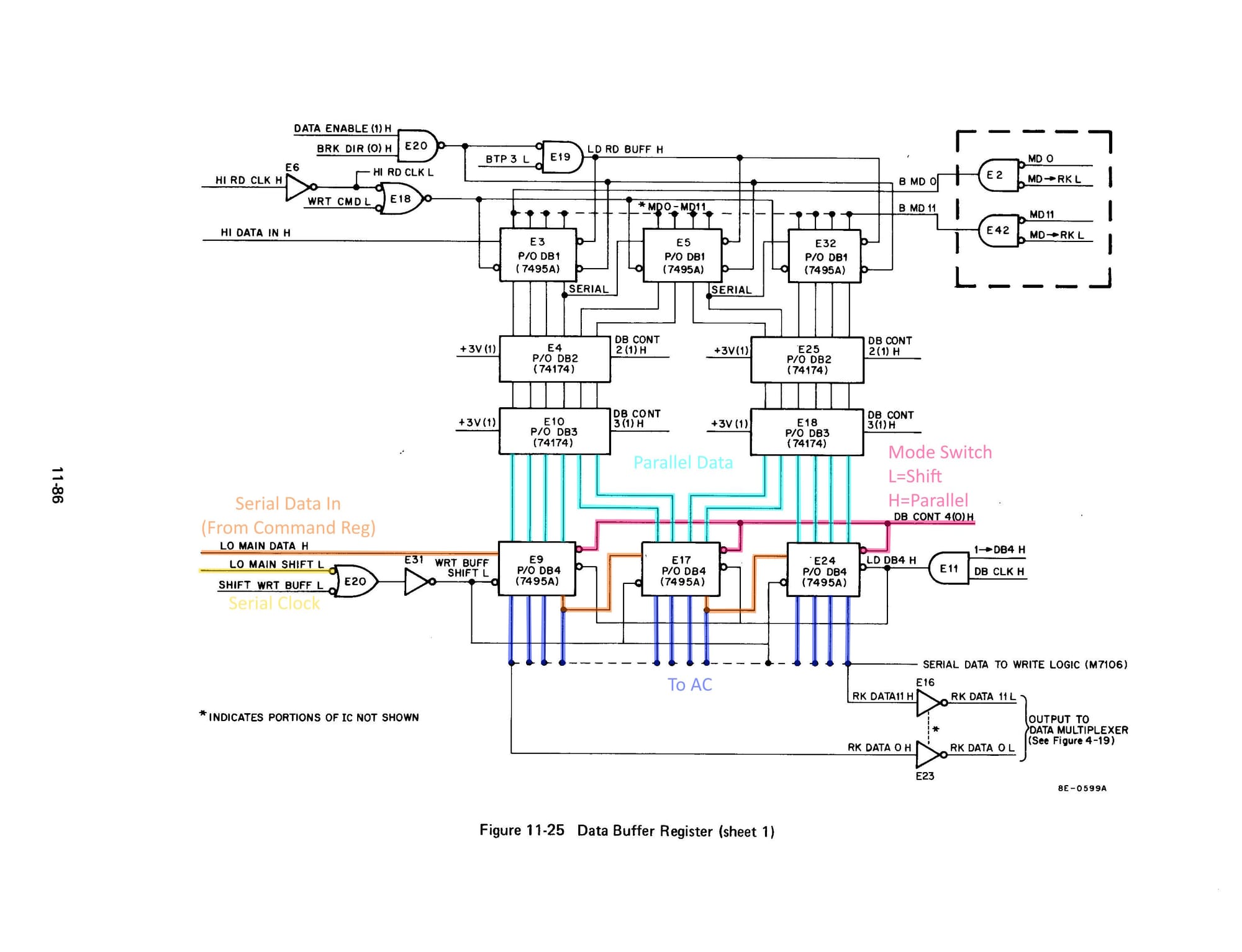
Initially, it looked like E9 had gone bad, so I swapped it with another. Unfortunately, that didn't solve the problem, and the E9 tested fine. I could see that 7777 was being latched into DB1-DB3; it was only data in DB4 that wasn't looking right.
With reasonable confidence that the registers were working correctly, I moved to the logic responsible for latching the registers. Because we know that data needs to make its way from DB1 to DB4, we should likely expect to see three pulses to propagate the data through the latches.
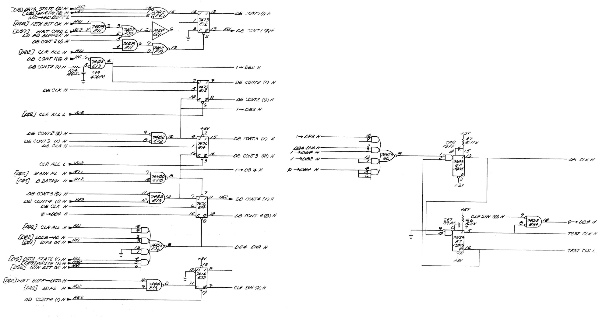
The circuit that produces the pulse chain to move the data is small but extremely complicated, consisting of 5 flip-flops and 2 monostable multivibrators.
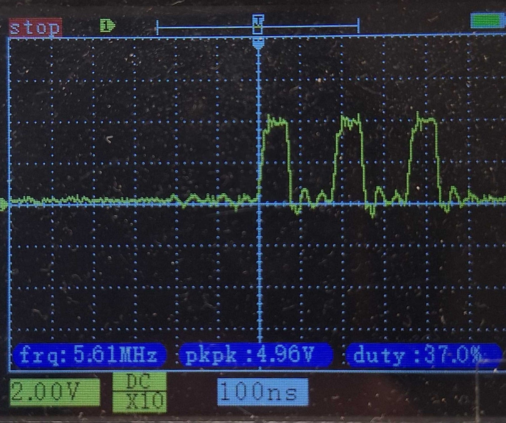
The output of this circuit, when it's working correctly, is three pulses. Comparing the defective board to a working board, I was able to see that one of the pulses was missing.
Because of the complexity and recursive nature of the circuit, it's extremely difficult to pinpoint which chip is not working correctly. In this case, the best approach is to connect each chip and turn to the logic analyser and compare it with a working board.
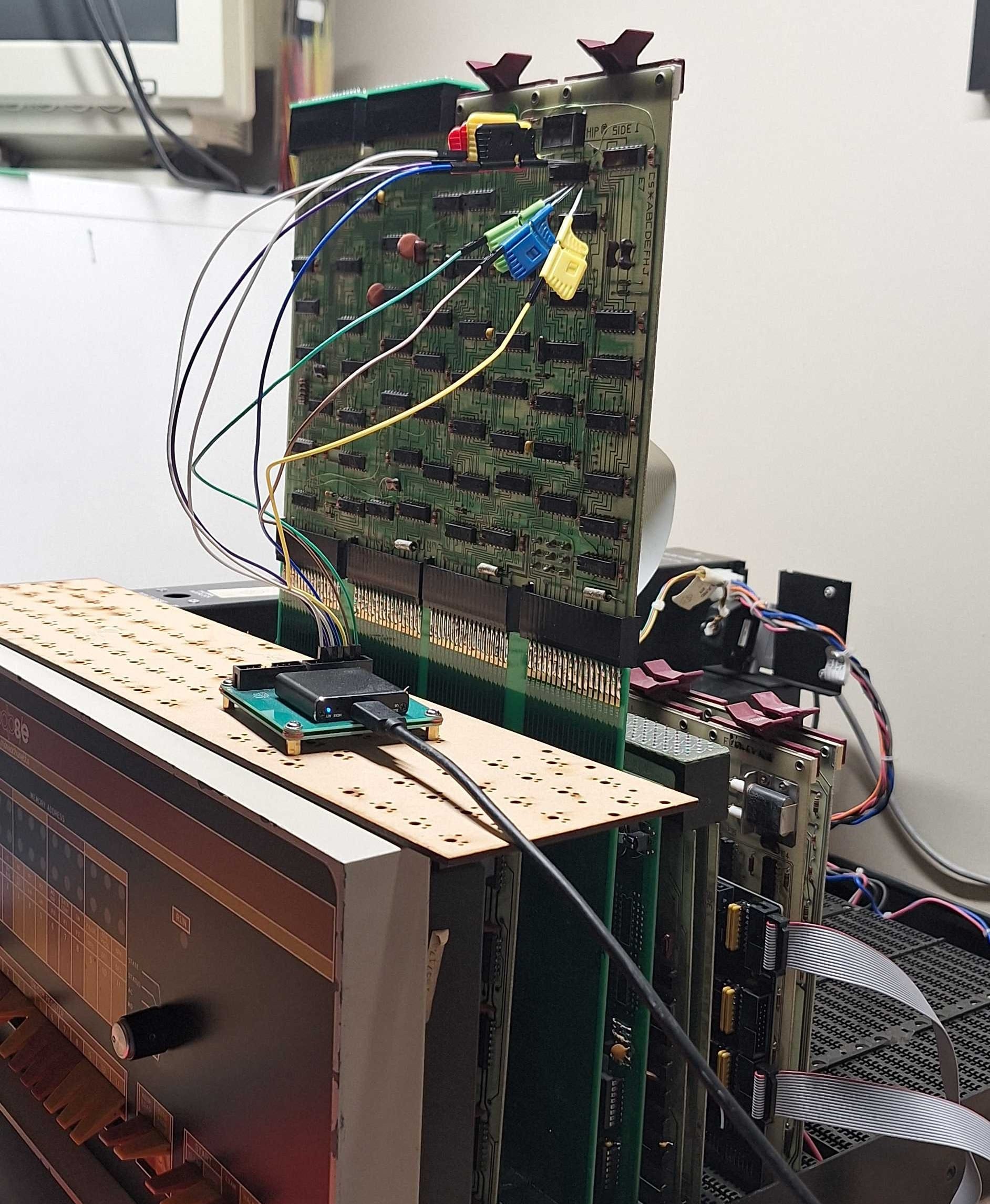
After 2 or 3 evenings of measuring and comparing chips, I was starting to narrow down the problem.
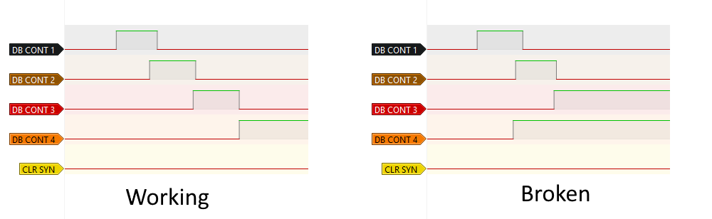
Putting the logic analyser on the flip-flop outputs, you can see that "DB CONT 3" is going high and remaining high, while "DB CONT 4" is going high too early. So the question is: Why do "DB CONT 3" & "DB CONT 4" not function as expected?
The next thing is to put the logic analyser onto the flip-flops that make up "DB CONT 3" & "DB CONT 4". That is exactly what I did.
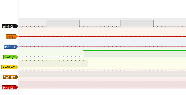
As it turns out, the second JK flip-flop (E14) was broken. From the above logic capture, you can see that the Q output, following the clock, goes high while J & K are LOW. This is the wrong behaviour for the JK flip-flop; it should have remained low. I replaced E14 (a 7476), and the board is now passing basic tests.
Successful Boot: 2026/10/3
Today, for the first time, the PDP-8/e booted its first operating system, OS8.
The working combination is as follows:
- M7104, Set 3
- M7105, Set 1
- M7106, Set 2
Board: M7106, Set 1 - 1:20s - 2026/10/4
DATA REGISTER ERROR
PC:1543 GD:7777 DB:0000

Expected value: 7777
Received value: 0000
This was a simple failure of E10, a 74H10. There is a counter that is responsible for deciding when to trigger the move from DB1 to DB2 etc. This is triggered after 12 clocks of the maintenance functions. In this case, the counter wasn't incrementing, and the DB buffers never got latched.
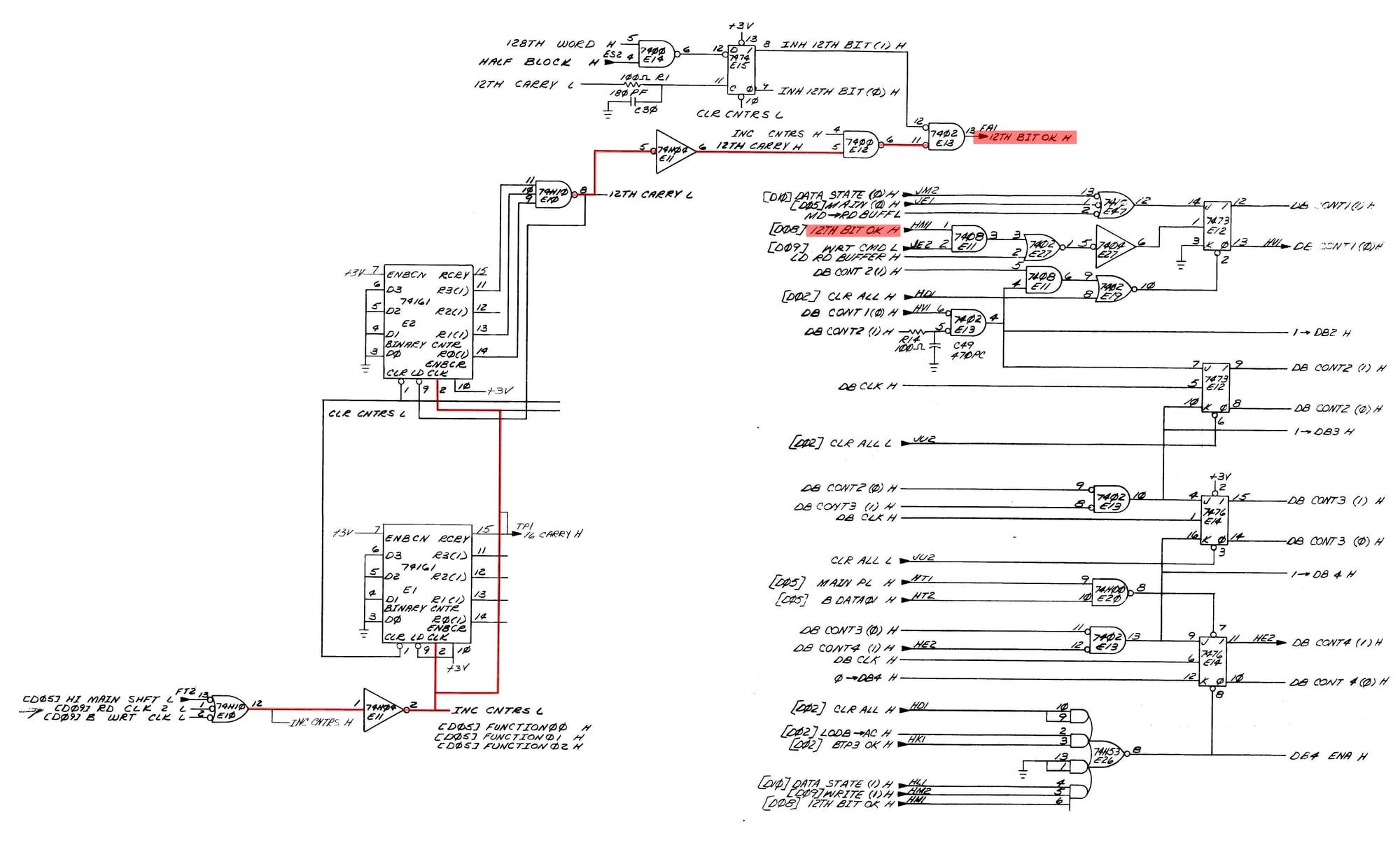
Board: M7104, Set 1 - 1:20s - 2026/10/4
DATA REGISTER ERROR
PC:1543 GD:0000 DB:7777

And

DATA REGISTER ERROR
PC:1543 GD:0000 DB:0077
Replaced E4 and E18