PDP-8/e Examine & Deposit Repair

For this PDP-8/e system, I have two sets of boards; one set is mostly functional, while the other set is only capable of loading addresses. All other console functions don't work. This includes examine and deposit.
Symptoms
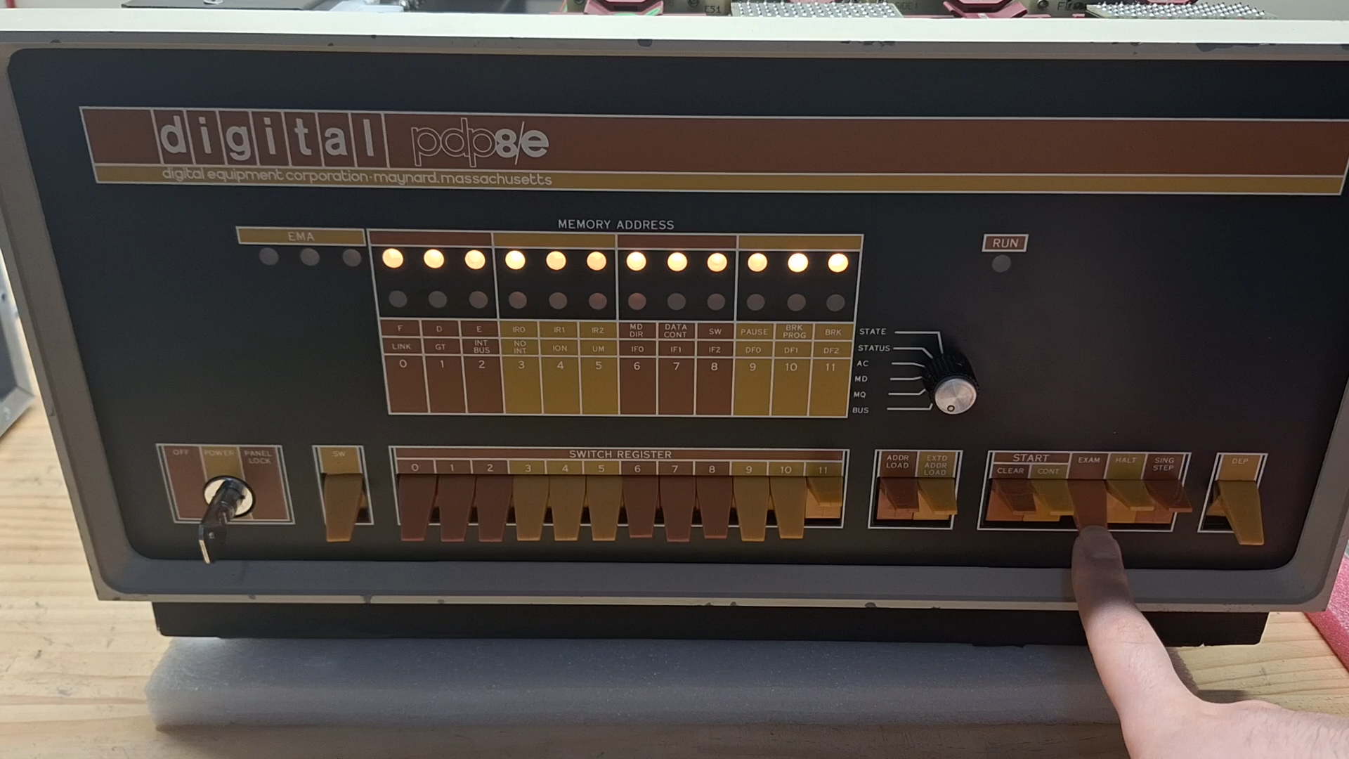
Pressing examine causes the wrong address to be loaded and no data is causes the wrong address to be loaded. This fault is isolated to M8310 – Major Control.
Questions
How does the data flow from the switch to the display and auto-increment?
What signals going into Major Control are important?
What signals coming out of Major Control are important?
Prerequisite Reading
Before we can start fixing any problems, we need to read up on the relevant documentation.
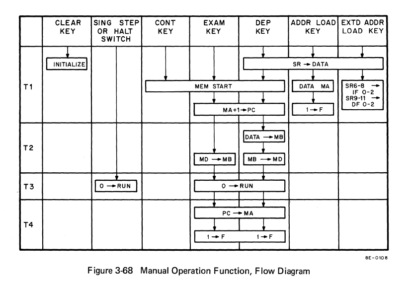
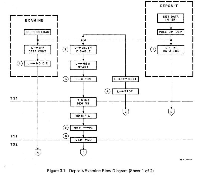
Examine Flow Explanation
1: Bus Set Up
Depressing the EXAM key asserts both BRK DATA CONT L and MD DIR L. These signals are necessary to read from memory and also allow the contents of the MD BUS to be applied to the MB Register.
BRK DATA CONT L is used to influence the state of EN1, one of the two select lines for the input register multiplexer.
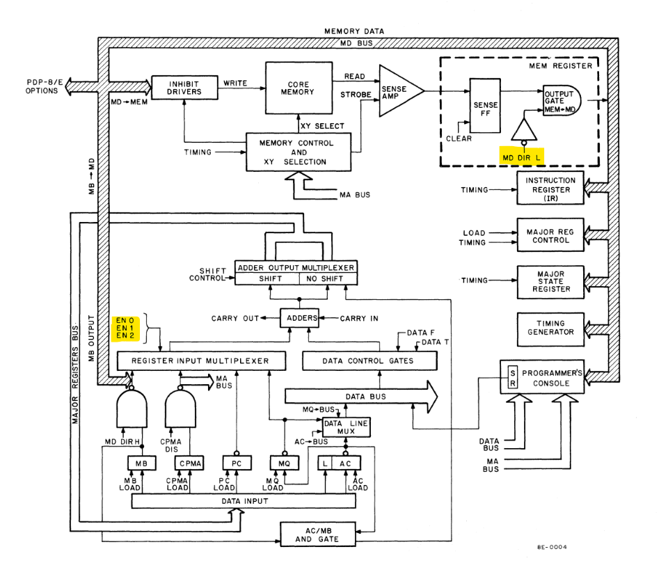
2: ALU Setup
The major states and Instruction Registers are disabled. Two control signals, MS, IR DISABLE L and KEY CONTROL L, are asserted.
MS, IR DISABLE L provides an arithmetic 0 at one input of the adder. This is done via the “Data Control Gates” selected by the DATA T and DATA F.
KEY CONTROL L is OR’ed with Buffered F to give BF + KC. In turn, BF + KC becomes EN0 if TS1 is also active. BF + KC also asserts carry in logic.
All of this provides the needed basic functionality to take the current address and increment it by one.
3: Timing Start
CONT, DEP, EXAM, switches trigger the assertion of the MEM START L. (KC8-EA)
Some milliseconds later (100us?), MEM START L is asserted, the RUN flip-flop is set, and a timing cycle begins. At TP1 time the PC Register is loaded with the next consecutive memory address (note that the nonincremented address remains in the CPMA Register until TP4 of the cycle).
The operator can activate either the DEP, CONT, or EXAM key, causing MEM START L to be asserted. This signal sets the RUN flip-flop; the 1 output of the flip-flop causes RUN L to be asserted and provides a high level at the D-input of flip-flop E39B. The next clock pulse sets E39B; the O-output of the flip-flop places IC E43 in the right-shift mode, and the timing cycle begins.
Testing
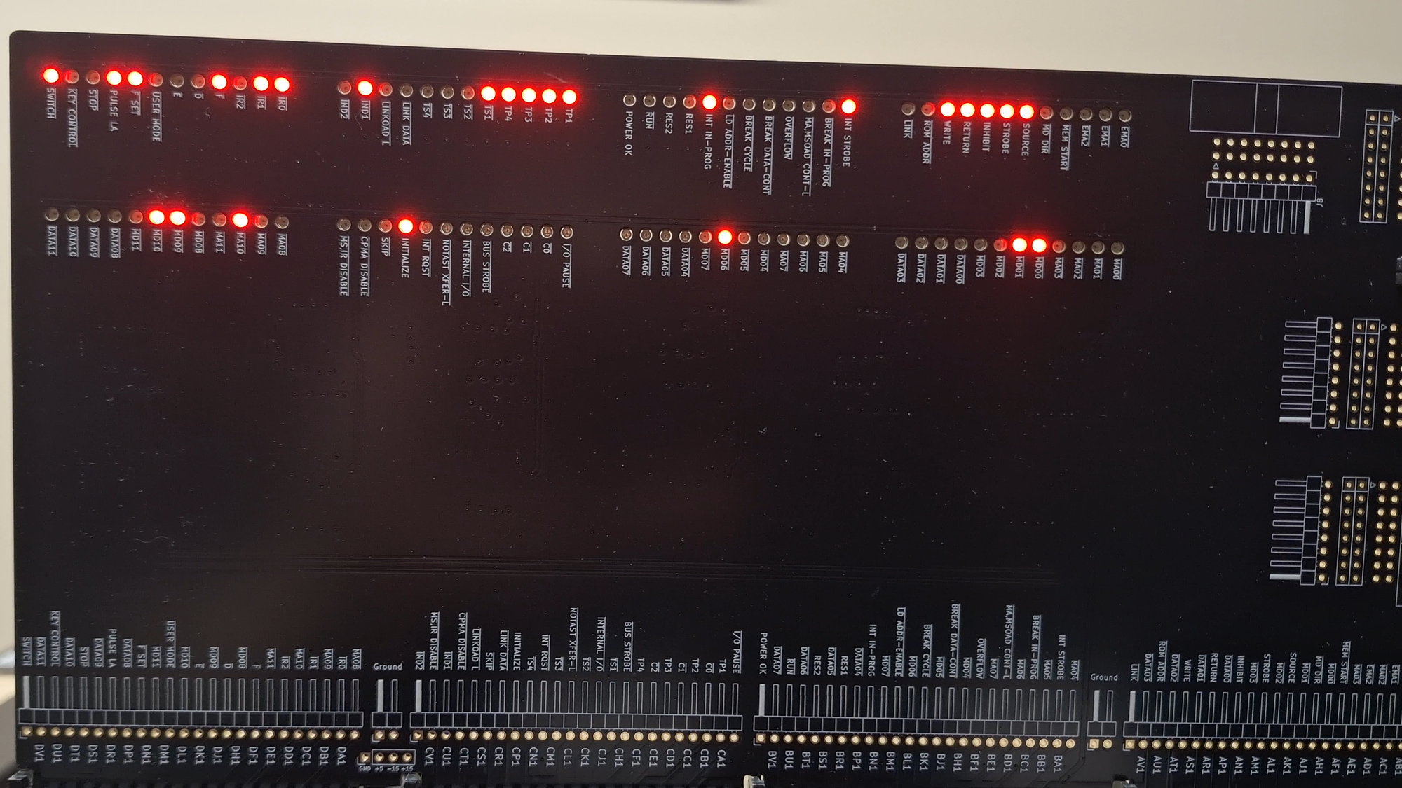
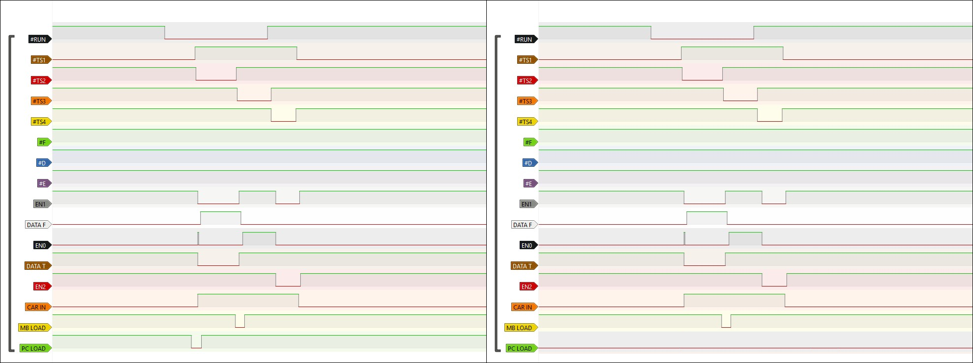
Having a reasonably good idea of how the system does address auto-incrementation, I decided it would be a perfect time to test out my newly built OmniProbe. I selected the following signals to look at:
RUN
TS1, TS2, TS3, Ts4
F, D, E
EF2 - EN1 - M8310
ED1 - DATA F - M8310
EC2 - EN0 - M8310
EB2 - DATA T - M8310
EA2 - EN2 - M8310
HM2 - CAR IN 12 - M8310
HF1 - MB LOAD L - M8310
HD1 - PC LOAD L - M8310
Analysis
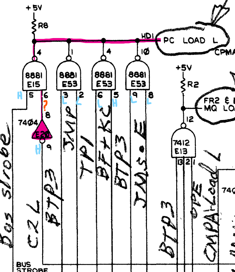
Taking a little bit of time to explore the logic captures and compare working boards to non-working boards, the problem became self-evident. On the broken board, PC LOAD was permanently asserted. It's used to latch MA + 1 into PC, one of the core functions of the auto-increment.
The Fix
Looking over the PC LOAD circuit, I quickly found that the NOT gate E20 was outputting 2V when its input was high. Checking a few other gates in the same chip strongly suggested that the 7404 (E20) had gone bad.
Replacing E20 restored examine and deposit functionality.